We have compiled a list of manufacturers, distributors, product information, reference prices, and rankings for Developing device.
ipros is IPROS GMS IPROS One of the largest technical database sites in Japan that collects information on.

Developing device Product List and Ranking from 24 Manufacturers, Suppliers and Companies | IPROS GMS

Last Updated: Aggregation Period:Feb 11, 2026~Mar 10, 2026
This ranking is based on the number of page views on our site.

Developing device Manufacturer, Suppliers and Company Rankings

Last Updated: Aggregation Period:Feb 11, 2026~Mar 10, 2026
This ranking is based on the number of page views on our site.

  1. エイ・エス・エイ・ピイ Saitama//Electronic Components and Semiconductors
  2. 富士フイルム 検査・測定 Tokyo//Testing, Analysis and Measurement
  3. 東京エレクトロン九州 Kumamoto//Electronic Components and Semiconductors
  4. 4 ラットコーポレーション 本社:営業部・業務部 Aichi//Trading company/Wholesale
  5. 5 カナメックス 厚木工場 Kanagawa//Electronic Components and Semiconductors

Developing device Product ranking

Last Updated: Aggregation Period:Feb 11, 2026~Mar 10, 2026
This ranking is based on the number of page views on our site.

  1. Non-destructive testing industrial X-ray film automatic developer 'FNDX 9A' 富士フイルム 検査・測定
  2. Tokyo Electron Kyushu Product Catalog 東京エレクトロン九州
  3. Static development type (paddle) automatic photoresist development device (developer) エイ・エス・エイ・ピイ
  4. 4 Automatic photoresist coating and developing equipment (coater-developer) エイ・エス・エイ・ピイ
  5. 5 2-fluid spray type automatic photoresist developing device (developer) エイ・エス・エイ・ピイ

Developing device Product List

1~30 item / All 51 items

Displayed results

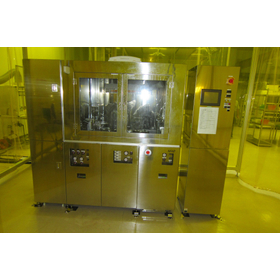
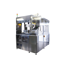
Development device "GX-40D"

A developing device that is easy to operate with a color LCD touch panel!

The "GX-40D" is a developing device that employs eight nozzle pipes, four on the top and four on the bottom, each capable of individual pressure adjustment. It is mainly suitable for applications such as the development of dry film resist and liquid resist in research and development. 【Features】 ■ Eight nozzle pipes on the top and bottom, each with individually adjustable pressure ■ Horizontal nozzle pipe oscillation ■ Easy operation with a color LCD touch panel ■ Automatically adjusts conveyor speed when the processing time for the chemical solution is input ■ Convenient height for side tank and drain port for easy handling of chemical solutions *For more details, please download the PDF or feel free to contact us.

  • Circuit board processing machine
  • Developing device

Added to bookmarks

Bookmarks list

Bookmark has been removed

Bookmarks list

You can't add any more bookmarks

By registering as a member, you can increase the number of bookmarks you can save and organize them with labels.

Free membership registration

Small Developer Machine SP Series SPD40

A design that combines user-friendly features with a sleek appearance.

The compact design ultra-high precision series SPseries SPD40 is a small developer that meets the needs for finer printed circuit boards as density increases. It is the definitive compact machine completed by utilizing the know-how of the Ninomiya system, including nozzle, nozzle arrangement, and oscillation. It features user-friendly functions and a sleek design with touch panel operation. Equipped with numerous safety features as standard, it allows for design modifications to meet customer needs. For more details, please contact us or refer to the catalog.

  • Other semiconductor manufacturing equipment
  • Developing device

Added to bookmarks

Bookmarks list

Bookmark has been removed

Bookmarks list

You can't add any more bookmarks

By registering as a member, you can increase the number of bookmarks you can save and organize them with labels.

Free membership registration

Liftoff (Image Reversal) Compatible Photoresist Development Equipment

Proven results with a variety of chemical solutions! The reason for our low prices is that we handle everything in-house, from design to sales.

The product is equipped with sheet-type development, front exposure (reverse exposure), baking, and cooling functions. We offer a lineup tailored to production volume, ranging from manual machines to fully automatic machines, and since we handle everything from design to manufacturing and sales in-house, we have achieved low prices. We have a proven track record with a variety of chemicals, including TMAH. 【Features】 ■ Achieves low prices ■ Automatic size recognition ■ Proven track record with a variety of chemicals ■ Reduced footprint ■ Lineup tailored to production volume *For more details, please refer to the PDF document or feel free to contact us.

  • Resist Device
  • Developing device

Added to bookmarks

Bookmarks list

Bookmark has been removed

Bookmarks list

You can't add any more bookmarks

By registering as a member, you can increase the number of bookmarks you can save and organize them with labels.

Free membership registration

1 Fluid Spray Type Automatic Photoresist Developer

It is a single-fluid developing device that is effective in reducing the development and processing time of thick films. You can freely choose the spray shape (circular, fan, etc.), pressure, and flow rate.

It is a single-fluid spray-type developing device. Since the spray is generated by the pressure of the developing solution, mist from the spray is less likely to scatter, and it can also speed up the developing process. It is optimal for developing large substrates and thick films. The spray nozzle can be freely selected in terms of shape (such as fan-shaped or circular), distribution, spreading angle, and range. This product is equipped with developing, baking, and cooling functions in a sheet-fed format. With a lineup tailored to production volume, ranging from manual machines to fully automatic machines, we have achieved low prices by handling everything from design to manufacturing and sales in-house. We have a proven track record with a variety of chemicals, including TMAH. 【Features】 ■ Equipped with single-fluid spray (can be used in conjunction with paddles) ■ Automatic wafer size recognition ■ Reduced footprint ■ Lineup tailored to production volume We have a demo setup available, so please consider scheduling a demonstration!

  • Resist Device
  • Developing device

Added to bookmarks

Bookmarks list

Bookmark has been removed

Bookmarks list

You can't add any more bookmarks

By registering as a member, you can increase the number of bookmarks you can save and organize them with labels.

Free membership registration

2-fluid spray type automatic photoresist developing device (developer)

From high pressure to mist-like soft pressure, it's all under control! A two-fluid spray resist development device. It is effective in shortening the development time for thick films and more.

This is a developing device that uses a two-fluid spray method to mix and discharge N2 and developer solution. By changing the pressure of N2, the discharge pressure of the spray can be adjusted. You can choose from a wide range of spray discharge patterns, such as increasing the liquid pressure for high-pressure discharge or reducing the liquid volume to create a fine mist for a softer discharge. The spray nozzle can be freely selected in various shapes such as fan-shaped or circular, as well as the distribution, spread angle, and range. We offer a lineup that matches production volume, from manual to fully automatic machines, and since we handle everything from design to manufacturing and sales in-house, we have achieved low prices. We have a proven track record with various chemicals, including TMAH. 【Features】 ■ Equipped with a two-fluid spray! (Paddle can also be used) ■ Automatic wafer size recognition function ■ Proven track record with various chemicals ■ Compact design ■ Lineup tailored to production volume We have a permanent demo setup, so please consider scheduling a demonstration!

  • Resist Device
  • Developing device

Added to bookmarks

Bookmarks list

Bookmark has been removed

Bookmarks list

You can't add any more bookmarks

By registering as a member, you can increase the number of bookmarks you can save and organize them with labels.

Free membership registration

Static development type (paddle) automatic photoresist development device (developer)

We have a proven track record with a variety of chemical solutions! The reason for our low prices is that we handle everything in-house, from design to sales.

The development is performed by pooling the developer solution on the wafer in a batch process. Unlike the dip method, each wafer is developed individually, resulting in very high reproducibility of the process. By optimizing the amount of chemical used, it leads to a reduction in the amount of developer solution used. We can accommodate requests for pooling methods, from shower types to straight nozzles. It also features a shaking function during static development! (It moves the liquid by repeating low rotation and stopping.) The batch process includes development, rinsing, baking, and cooling functions. We design, manufacture, and sell according to customer needs and production volumes. We have a proven track record with various chemicals, including TMAH. 【Features】 ■ High reproducibility of development results ■ Reduction in chemical usage ■ Automatic wafer size recognition ■ Proven track record with various chemicals ■ Reduced footprint ■ Design tailored to production volume We have a permanent demo setup, so please consider a demonstration!

  • Resist Device
  • Developing device

Added to bookmarks

Bookmarks list

Bookmark has been removed

Bookmarks list

You can't add any more bookmarks

By registering as a member, you can increase the number of bookmarks you can save and organize them with labels.

Free membership registration

Automatic photoresist coating and developing equipment (coater-developer)

Compatible with low to high viscosity resists! We can manufacture equipment for any wafer size, from small diameter to large diameter!

【Features】 ■ Achieves low price ■ Supports low to high viscosity (1.7cP to 10000cP) ■ Compatible with sizes from 2 to 12 inches ■ Capable of processing multiple wafer sizes (e.g., compatible with 3, 4, 5 inches and 8, 12 inches) ■ Automatic wafer size recognition system ■ Proven performance with a variety of chemicals ■ Reduced footprint (space-saving) ■ Numerous options available with resist reduction ■ Lineup tailored to production volume 【ASAP Coater/Developer Functions】 ● Spin coating ● HMDS treatment ● Baking ● Cooling ● Developing ● Rinsing We have achieved low prices by handling everything from design to manufacturing and sales in-house! 【ASAP Features and Achievements】 ● Proven use of a variety of chemicals including positive and negative resists, polyimide, SOG, WAX, silicone, etc. ● Extensive experience in substrate transport including Si (silicon), GaAs, InP, GaN, SiC, sapphire, ceramics, SiO2 (glass), etc. ● Numerous transport achievements with thin substrates such as GaAs (thickness 150um), InP (thickness 150um), LT (thickness 120um)! *For more details, please refer to the PDF document or feel free to contact us.

  • Coater
  • Resist Device
  • Other semiconductor manufacturing equipment
  • Developing device

Added to bookmarks

Bookmarks list

Bookmark has been removed

Bookmarks list

You can't add any more bookmarks

By registering as a member, you can increase the number of bookmarks you can save and organize them with labels.

Free membership registration

Spin cleaning device, spray developing device

Demo units available for loan! You can process several sheets at once.

This machine is a spin-type spray developing device that performs developing, rinsing, washing, and drying through automatic and manual operation. It can process several workpieces at once. For more details, please contact us or refer to the catalog.

  • Other semiconductor manufacturing equipment
  • Developing device

Added to bookmarks

Bookmarks list

Bookmark has been removed

Bookmarks list

You can't add any more bookmarks

By registering as a member, you can increase the number of bookmarks you can save and organize them with labels.

Free membership registration

Organic solvent-based spray developing device WSD-150

Device dimensions: 560W × 850D × 1300H

Set the substrate in the chuck manually, then perform spray development, rinsing, and spin drying.

  • Other semiconductor manufacturing equipment
  • Developing device

Added to bookmarks

Bookmarks list

Bookmark has been removed

Bookmarks list

You can't add any more bookmarks

By registering as a member, you can increase the number of bookmarks you can save and organize them with labels.

Free membership registration

Single-sheet spin developing machine WSD-200CBT/WSD-300CBT

Device dimensions: 1200W × 1100D × 2000H (200CBT) / 1500W × 1100D × 2000H (300CBT)

Set the substrate in the chuck manually, then perform paddle development, rinsing, and spin drying.

  • Other semiconductor manufacturing equipment
  • Developing device

Added to bookmarks

Bookmarks list

Bookmark has been removed

Bookmarks list

You can't add any more bookmarks

By registering as a member, you can increase the number of bookmarks you can save and organize them with labels.

Free membership registration

Coating and Developing Equipment ACS300 Gen2

Type up to 300mm - Spin Coating/Developing Cluster

Wafer-level packaging for mass production and 3D integration.

  • Other processing machines
  • Developing device

Added to bookmarks

Bookmarks list

Bookmark has been removed

Bookmarks list

You can't add any more bookmarks

By registering as a member, you can increase the number of bookmarks you can save and organize them with labels.

Free membership registration

Semiconductor printed circuit board horizontal manufacturing equipment for solder resist development (finishing process)

Supports everything from single-layer substrates to flexible substrates using Roll to Roll! No resist residue remains.

We would like to introduce the solder resist development for finishing treatment handled by Fujikiko Co., Ltd. It accommodates everything from single-sided PCBs to flexible PCBs using Roll to Roll. Additionally, due to optimal spray placement, there is no residue left from the resist. 【Features】 ■ Accommodates everything from single-sided PCBs to flexible PCBs using Roll to Roll ■ Optimal spray placement ■ No resist residue left *For more details, please refer to the PDF document or feel free to contact us.

  • Other semiconductor manufacturing equipment
  • Other surface treatment equipment
  • Circuit board processing machine
  • Developing device

Added to bookmarks

Bookmarks list

Bookmark has been removed

Bookmarks list

You can't add any more bookmarks

By registering as a member, you can increase the number of bookmarks you can save and organize them with labels.

Free membership registration

Development device

Achieve uniform development processing with a unique spray array! Introducing a development device with excellent maintenance characteristics.

This product is a patterning development device after exposure processing. Thanks to our unique spray arrangement, uniform development processing is achieved. We have adopted transport rolls that are less prone to slipping, which reduces damage to the resist caused by product waviness. Additionally, the lid of the development chamber opens wide, providing excellent maintenance accessibility. 【Features】 ■ Capable of uniform development processing ■ Adoption of transport rolls that are less prone to slipping ■ Reduces damage to the resist caused by product waviness ■ High maintenance accessibility *For more details, please refer to the PDF document or feel free to contact us.

  • Wafer
  • Other surface treatment equipment
  • Developing device

Added to bookmarks

Bookmarks list

Bookmark has been removed

Bookmarks list

You can't add any more bookmarks

By registering as a member, you can increase the number of bookmarks you can save and organize them with labels.

Free membership registration

Non-contact D/F developer

The precision of the transport fixture is high! The knife connection part is of the socket type, making disassembly and installation very easy.

This product is a non-contact D/F developer with high precision in transport fixtures and easy maintenance. The use of Wind Jet and PATA-GUN nozzles improves the drying capability of the JIG Clamp section. Lightweight and standard products are used for KnifeAL injection items. Each Knife allows for pressure adjustment, and a pressure gauge is installed on the operation side for easy visual management. 【Features】 ■ Use of Wind Protector & PCB Clamp for high-speed operation ■ Installation of a sensing sensor to detect the presence or absence of the substrate during clamping ■ Application of an ALIGN System to prevent issues during product loading, even with misalignment or irregular input ■ Application of two upper FFUs for particle initialization (Option) ■ Driven by LD/ULD & 6-axis articulated robot with PLC control *For more details, please refer to the PDF materials or feel free to contact us.

Added to bookmarks

Bookmarks list

Bookmark has been removed

Bookmarks list

You can't add any more bookmarks

By registering as a member, you can increase the number of bookmarks you can save and organize them with labels.

Free membership registration

Tokyo Electron Kyushu Product Catalog

Featuring the latest products from Tokyo Electron Kyushu, a leading company in semiconductor manufacturing equipment!

The "Tokyo Electron Kyushu Product Guide" is a comprehensive catalog from Tokyo Electron Kyushu, which conducts research, development, and design of semiconductor manufacturing equipment and EPD manufacturing equipment. It features a number of the latest semiconductor coating and developing equipment along with detailed explanations. Additionally, it introduces trends in the current semiconductor coating and developing equipment research projects, as well as the development projects for semiconductor cleaning equipment. Currently, the product guide is being offered for free. [Contents] ■ Semiconductor Coating and Developing Equipment ■ Semiconductor Cleaning Equipment ■ Wafer Bonding Equipment ■ FPD Coater ■ Introduction to Research and Development of Various Semiconductor Manufacturing Equipment *For more details, please refer to the catalog or feel free to contact us.

  • Other semiconductor manufacturing equipment
  • Developing device

Added to bookmarks

Bookmarks list

Bookmark has been removed

Bookmarks list

You can't add any more bookmarks

By registering as a member, you can increase the number of bookmarks you can save and organize them with labels.

Free membership registration

Spray Development Device for Printed Circuit Boards

New technology for developing printed circuit boards!

Asahi Electric Materials Co., Ltd. offers a "Mist Development System for Printed Circuit Boards" with a unique air slit structure that produces high directivity in the developer solution. Due to the high-pressure misting of the developer solution, deep etching (high aspect ratio) is possible. Unlike liquid, the mist form makes it less likely to form liquid droplets, improving surface uniformity and stabilizing quality. Additionally, since the amount of developer solution used is minimal, development can be carried out with only fresh solution without liquid circulation, and no defoamer is needed, eliminating concerns about issues like sludge. 【Features】 ■ Development time is reduced to less than one-third, improving productivity. ■ The line length is reduced to less than half, allowing for effective use of the equipment installation area. *For more details, please download the PDF or feel free to contact us.

  • Other markings
  • Other image-related equipment
  • Developing device

Added to bookmarks

Bookmarks list

Bookmark has been removed

Bookmarks list

You can't add any more bookmarks

By registering as a member, you can increase the number of bookmarks you can save and organize them with labels.

Free membership registration

Symbolic Tech Film Automatic Developer

Equipped with seven programmable process channels that have sufficient flexibility.

The "Symbolic Tech Film Automatic Development Machine" is a device that consolidates all the experience and technology cultivated in PCB film automatic development technology. The intermediate washing system has a take-up roller and performs film cleanup to minimize the carryover of chemicals to the next process. Additionally, the crossover roller that transfers to the next process is positioned above the liquid level and is designed for easy removal and cleaning. 【Standard Features and Accessories】 ■ Removable feed table ■ Upgradeable to higher production capacity at the user site ■ Monitoring of developer liquid levels ■ External filters for development, fixing, and washing ■ Filter replacement timing notification alarm ■ Automatic standby and low power mode ■ Monitoring function *For more details, please download the PDF or feel free to contact us.

  • Other image-related equipment
  • Developing device

Added to bookmarks

Bookmarks list

Bookmark has been removed

Bookmarks list

You can't add any more bookmarks

By registering as a member, you can increase the number of bookmarks you can save and organize them with labels.

Free membership registration

Leaf-type spin developing device

Automatic processing of each step from paddle development, spray development, rinsing, to spin drying!

We would like to introduce the "Sheet-Type Spin Developer" that we handle. By simply setting the cassette in the loader, the clean robot automatically transports the workpiece and processes each step automatically. For developing large substrates, we recommend the coating method. In the manual type, the workpiece can be manually set in the chuck, and similar developing, rinsing, and spin-drying processes can be performed. 【Specifications (partial)】 ■ Work Material - Si, SiC, GaN, GaAs, InP, LT/LN, ceramics, quartz, resin, glass, etc. ■ Developer: TMAH, Na2CO3, cyclopentane (independent chamber) ■ Rinse Liquid: DIW, PGMEA, etc. ■ Back Rinse: PGMEA, etc. ■ Coating Method: Shower or nozzle *For more details, please download the PDF or feel free to contact us.

  • 枚葉式スピン現像装置2.png
  • 枚葉式スピン現像装置3.png
  • Other cleaning machines
  • Developing device

Added to bookmarks

Bookmarks list

Bookmark has been removed

Bookmarks list

You can't add any more bookmarks

By registering as a member, you can increase the number of bookmarks you can save and organize them with labels.

Free membership registration

Developing equipment for ceramic substrates

Development equipment for ceramic substrates

We contribute to enhancing our customers' added value by utilizing advanced fine processing technology for developing and etching, as well as advanced thin plate transport technology.

  • Other mounting machines
  • Developing device

Added to bookmarks

Bookmarks list

Bookmark has been removed

Bookmarks list

You can't add any more bookmarks

By registering as a member, you can increase the number of bookmarks you can save and organize them with labels.

Free membership registration

Ninomiya System Glass Substrate Development Equipment

Ninomiya System Glass Substrate Development Equipment

Achieving high-precision development through optimal nozzle arrangement.

  • Other semiconductor manufacturing equipment
  • Developing device

Added to bookmarks

Bookmarks list

Bookmark has been removed

Bookmarks list

You can't add any more bookmarks

By registering as a member, you can increase the number of bookmarks you can save and organize them with labels.

Free membership registration

Compact! Manual photoresist developing device (manual developer)

It is a compact resist development system for small-lot, multi-variety production and development applications. Unlike DIP, it can stabilize quality due to its sheet-fed design.

This product is a manual sheet-type developing machine. It features a compact design that combines the chemical solution box and processing cup into one unit. We design, manufacture, and sell manual machines tailored to our customers' needs. It is used not only for research and development purposes but also by customers handling small quantities of diverse products. We have a proven track record with various chemicals, including TMAH. 【Features】 ■ Achieves low cost ■ Compact! ■ Options for paddle, single fluid spray, and dual fluid spray ■ Proven performance with a variety of chemicals *For more details, please refer to the PDF document or feel free to contact us.

  • Resist Device
  • Developing device

Added to bookmarks

Bookmarks list

Bookmark has been removed

Bookmarks list

You can't add any more bookmarks

By registering as a member, you can increase the number of bookmarks you can save and organize them with labels.

Free membership registration

Maintain a constant reverse taper angle! PEB-compatible resist development equipment (developer)

Keep the negative taper angle constant! This is an automatic resist development system compatible with post-exposure bake (PEB) required for negative resist and image reversal resist.

Equipped with sheet-type development, full exposure (inverted exposure, image reversal), baking, and cooling functions. An important PEB that determines the angle of the reverse taper using lift-off resist. Our proprietary program stabilizes the reverse taper angle! Additionally, using it for baking after exposing negative resist achieves a stable process. With a lineup tailored to production volume, from manual machines to fully automatic machines, we have realized low prices by handling everything from design to manufacturing and sales in-house. We have a proven track record with a variety of chemicals such as TMAH, colin aqueous solution, and Na2CO3. We also have numerous achievements with thin wafers (such as wafer thickness of 150um), so please feel free to consult us. 【Features】 ■ Stability of reverse taper angle through PEB ■ Automatic wafer size recognition function ■ Compatible with paddle, single-fluid spray, and dual-fluid spray ■ Reduced footprint ■ Lineup tailored to production volume We also have demo equipment available, so please consider scheduling a demonstration!

  • Resist Device
  • Developing device

Added to bookmarks

Bookmarks list

Bookmark has been removed

Bookmarks list

You can't add any more bookmarks

By registering as a member, you can increase the number of bookmarks you can save and organize them with labels.

Free membership registration

Automatic resist coating and developing equipment for corner substrates (coater-developer)

Supports low to high viscosity resist! Equipment can be manufactured for any wafer size!

The product is equipped with spin coating, HMDS treatment, baking, and cooling functions. Since we handle everything from design to manufacturing and sales in-house, we have achieved low prices! We have a proven track record with a variety of chemicals including positive-negative resist, polyimide, SOG, wax, and silicone. We also have extensive experience in transporting various substrates such as Si (silicon), GaAs, InP, GaN, SiC, sapphire, and ceramic, as well as SiO2 (glass). We have numerous achievements in transporting thin substrates and square substrates, such as GaAs (thickness 150um), InP (thickness 150um), and LT (thickness 120um)! 【Features】 ■ Achieves low prices ■ Capable of handling low to high viscosity (1.7cP to 10000cP) ■ Uniform film distribution through a rotating cup coating method ■ Compatible with 2 to 12 inches ■ Capable of processing multiple types of wafers (compatible with 3, 4, and 5 inches) ■ Automatic recognition of wafer size ■ Proven track record with a variety of chemicals ■ Reduced footprint (space-saving) ■ Numerous options for resist reduction ■ Lineup tailored to production volume *For more details, please refer to the PDF document or feel free to contact us.

  • Coater
  • Developing device

Added to bookmarks

Bookmarks list

Bookmark has been removed

Bookmarks list

You can't add any more bookmarks

By registering as a member, you can increase the number of bookmarks you can save and organize them with labels.

Free membership registration

Spin Cleaning Device Spray Development Device SD-8004 Type

Automatic and manual operation will perform developing, rinsing, washing, and spin drying!

The SD-8004 model is a spin spray development system for 4" to 8" wafers. It performs developing, rinsing, water washing, and spin drying through automatic and manual operation. Condition settings are done via a touch panel on the operation panel. Each processing mode is displayed on the touch panel during the respective mode. For more details, please contact us or refer to the catalog.

  • Coater
  • Other semiconductor manufacturing equipment
  • Developing device

Added to bookmarks

Bookmarks list

Bookmark has been removed

Bookmarks list

You can't add any more bookmarks

By registering as a member, you can increase the number of bookmarks you can save and organize them with labels.

Free membership registration

Small developing device for photolithography

Small developing device for photolithography

Swing nozzle type spray development and paddle development compatible device 【Features】 - High performance, low price, compact tabletop type - Work size Φ1" to Φ6" - Easy operation with program input via LCD touch panel - Built-in dual liquid pressure delivery pumps ◆ For detailed specifications, refer to the catalog ◆

  • Etching Equipment
  • Developing device

Added to bookmarks

Bookmarks list

Bookmark has been removed

Bookmarks list

You can't add any more bookmarks

By registering as a member, you can increase the number of bookmarks you can save and organize them with labels.

Free membership registration

Organic solvent-based spin development device WSD-200T

Device dimensions: 1700W × 1300D × 1400H

Set the substrate manually in the chuck, then perform paddle development, rinsing, and spin drying. A canister can be stored on the side of the main unit.

  • Other semiconductor manufacturing equipment
  • Developing device

Added to bookmarks

Bookmarks list

Bookmark has been removed

Bookmarks list

You can't add any more bookmarks

By registering as a member, you can increase the number of bookmarks you can save and organize them with labels.

Free membership registration

Fully automatic screen printing processor

Fully automatic screen printing developing machine

As a manufacturer of screen printing machines, we have created screen plate processing equipment that embodies our commitment and experience in screen plates. Traditionally, the development process of screen plates after exposure has been done manually using spray guns and other tools. However, due to the recent refinement of printing patterns and the increase in screen plate sizes, meeting the required quality for plate making has become increasingly difficult. That’s why we recommend the Mino Screen Processor 2! This is a renewed version of the popular Mino Screen Processor, now equipped with more user-friendly specifications. Its uniform and powerful cleaning capability, unique to fully automatic operation, ensures high plate making accuracy. Additionally, it comes standard with a backlight, making it easy to check for any gaps in the plate. The standard-equipped sash door prevents cleaning noise and leakage of developing water, ensuring a comfortable working environment. By recycling the developing water, it also helps reduce costs and lessen the environmental impact.

  • Other processing machines
  • Developing device

Added to bookmarks

Bookmarks list

Bookmark has been removed

Bookmarks list

You can't add any more bookmarks

By registering as a member, you can increase the number of bookmarks you can save and organize them with labels.

Free membership registration

Coating and Developing Equipment ACS200

Fully automatic, compatible with a maximum of 200mm.

By docking our mask aligner module with the full-area exposure method, it can be used as the Ring Graphy Cluster LithoFab200.

  • Other processing machines
  • Developing device

Added to bookmarks

Bookmarks list

Bookmark has been removed

Bookmarks list

You can't add any more bookmarks

By registering as a member, you can increase the number of bookmarks you can save and organize them with labels.

Free membership registration

Development device

Development process after exposure of wiring patterns! Introduction of development equipment powered by AC 200V/220V, 50Hz/60Hz.

We would like to introduce our "Developing Equipment." This equipment is capable of developing after the exposure of wiring patterns. The processing surfaces can be single-sided or double-sided. The equipment configuration includes unwinding, developing, rinsing, liquid removal, drying, and winding. 【Specifications】 ■ Lane configuration: 2 Lanes ■ Transport speed: 2.0 m/min ■ Material width: 35mm to 160mm for TAB/CSP/COF (250mm to 300mm for FPC) ■ Material thickness: PI 25μm and above ■ Processing surface: Single-sided and double-sided *For more details, please refer to the PDF document or feel free to contact us.

  • Drying Equipment
  • Image Processing Equipment
  • Developing device

Added to bookmarks

Bookmarks list

Bookmark has been removed

Bookmarks list

You can't add any more bookmarks

By registering as a member, you can increase the number of bookmarks you can save and organize them with labels.

Free membership registration